- 您现在的位置:买卖IC网 > Sheet目录1905 > ATMEGA649V-8MI (Atmel)IC AVR MCU FLASH 64K 1.8V 64QFN
PIC16(L)F1825/1829
DS41440C-page 292
2010-2012 Microchip Technology Inc.
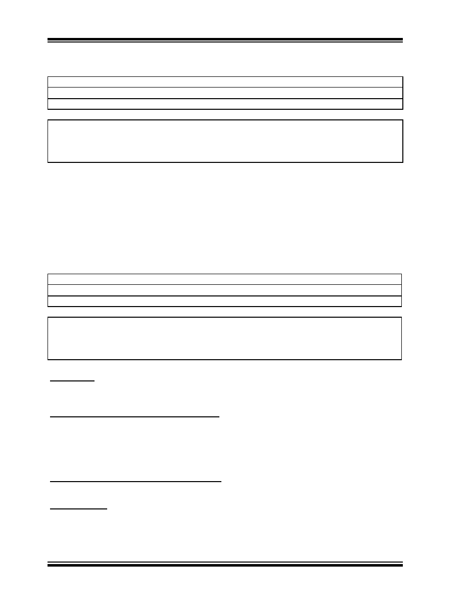
REGISTER 25-5:
SSPMSK: SSPx MASK REGISTER
R/W-1/1
MSK<7:0>
bit 7
bit 0
Legend:
R = Readable bit
W = Writable bit
U = Unimplemented bit, read as ‘0’
u = Bit is unchanged
x = Bit is unknown
-n/n = Value at POR and BOR/Value at all other Resets
‘1’ = Bit is set
‘0’ = Bit is cleared
bit 7-1
MSK<7:1>:
Mask bits
1 = The received address bit n is compared to SSPxADD<n> to detect I2C address match
0 = The received address bit n is not used to detect I2C address match
bit 0
MSK<0>:
Mask bit for I2C Slave mode, 10-bit Address
I2C Slave mode, 10-bit address (SSPM<3:0> = 0111 or 1111):
1 = The received address bit 0 is compared to SSPxADD<0> to detect I2C address match
0 = The received address bit 0 is not used to detect I2C address match
I2C Slave mode, 7-bit address, the bit is ignored
REGISTER 25-6:
SSPxADD: MSSPx ADDRESS AND BAUD RATE REGISTER (I2C MODE)
R/W-0/0
ADD<7:0>
bit 7
bit 0
Legend:
R = Readable bit
W = Writable bit
U = Unimplemented bit, read as ‘0’
u = Bit is unchanged
x = Bit is unknown
-n/n = Value at POR and BOR/Value at all other Resets
‘1’ = Bit is set
‘0’ = Bit is cleared
Master mode:
bit 7-0
ADD<7:0>:
Baud Rate Clock Divider bits
SCLx pin clock period = ((ADD<7:0> + 1) *4)/FOSC
10-Bit Slave mode — Most Significant Address byte:
bit 7-3
Not used:
Unused for Most Significant Address byte. Bit state of this register is a “don’t care”. Bit
pattern sent by master is fixed by I2C specification and must be equal to ‘11110’. However, those bits
are compared by hardware and are not affected by the value in this register.
bit 2-1
ADD<2:1>:
Two Most Significant bits of 10-bit address
bit 0
Not used:
Unused in this mode. Bit state is a “don’t care”.
10-Bit Slave mode — Least Significant Address byte:
bit 7-0
ADD<7:0>:
Eight Least Significant bits of 10-bit address
7-Bit Slave mode:
bit 7-1
ADD<7:1>:
7-bit address
bit 0
Not used:
Unused in this mode. Bit state is a “don’t care”.
发布紧急采购,3分钟左右您将得到回复。
相关PDF资料
ATMEGA8515L-8JUR
MCU AVR 8KB FLASH 8MHZ 44PLCC
ATMEGA8515L-8PJ
IC MCU AVR 8K 5V 8MHZ 40-DIP
ATMEGA8535-16JUR
MCU AVR 8K FLASH 16MHZ 44PLCC
ATMEGA8535L-8PJ
IC MCU AVR 8K 5V 8MHZ 40-DIP
ATMEGA88-15MT2
MCU AVR 8K FLASH 15MHZ 32-QFN
ATMEGA88-20AUR
MCU AVR 8K FLASH 20MHZ 32TQFP
ATMEGA88P-20AUR
MCU AVR 8KB FLASH 20MHZ 32TQFP
ATMEGA8HVA-4CKU
MCU AVR 8K FLASH 4MHZ 36-LGA
相关代理商/技术参数
ATmega649V-8MU
功能描述:8位微控制器 -MCU AVR 64K FLASH 2K EE 4K SRAM ADC LCD RoHS:否 制造商:Silicon Labs 核心:8051 处理器系列:C8051F39x 数据总线宽度:8 bit 最大时钟频率:50 MHz 程序存储器大小:16 KB 数据 RAM 大小:1 KB 片上 ADC:Yes 工作电源电压:1.8 V to 3.6 V 工作温度范围:- 40 C to + 105 C 封装 / 箱体:QFN-20 安装风格:SMD/SMT
ATMEGA649V-8MUR
功能描述:8位微控制器 -MCU AVR 64KB FLSH 2KB EE 4KB SRAM LCD8MHz1.8V RoHS:否 制造商:Silicon Labs 核心:8051 处理器系列:C8051F39x 数据总线宽度:8 bit 最大时钟频率:50 MHz 程序存储器大小:16 KB 数据 RAM 大小:1 KB 片上 ADC:Yes 工作电源电压:1.8 V to 3.6 V 工作温度范围:- 40 C to + 105 C 封装 / 箱体:QFN-20 安装风格:SMD/SMT
ATMEGA64A-AN
功能描述:8位微控制器 -MCU 16MHz 105C RoHS:否 制造商:Silicon Labs 核心:8051 处理器系列:C8051F39x 数据总线宽度:8 bit 最大时钟频率:50 MHz 程序存储器大小:16 KB 数据 RAM 大小:1 KB 片上 ADC:Yes 工作电源电压:1.8 V to 3.6 V 工作温度范围:- 40 C to + 105 C 封装 / 箱体:QFN-20 安装风格:SMD/SMT
ATMEGA64A-ANR
功能描述:8位微控制器 -MCU 16MHz 105C RoHS:否 制造商:Silicon Labs 核心:8051 处理器系列:C8051F39x 数据总线宽度:8 bit 最大时钟频率:50 MHz 程序存储器大小:16 KB 数据 RAM 大小:1 KB 片上 ADC:Yes 工作电源电压:1.8 V to 3.6 V 工作温度范围:- 40 C to + 105 C 封装 / 箱体:QFN-20 安装风格:SMD/SMT
ATMEGA64A-AU
功能描述:8位微控制器 -MCU 64K Flsh 2K EEPROM 4K SRAM 16MHz RoHS:否 制造商:Silicon Labs 核心:8051 处理器系列:C8051F39x 数据总线宽度:8 bit 最大时钟频率:50 MHz 程序存储器大小:16 KB 数据 RAM 大小:1 KB 片上 ADC:Yes 工作电源电压:1.8 V to 3.6 V 工作温度范围:- 40 C to + 105 C 封装 / 箱体:QFN-20 安装风格:SMD/SMT
ATMEGA64A-AUR
功能描述:8位微控制器 -MCU AVR 64KB FLSH 2KB EE 4KB SRAM-16MHz IND RoHS:否 制造商:Silicon Labs 核心:8051 处理器系列:C8051F39x 数据总线宽度:8 bit 最大时钟频率:50 MHz 程序存储器大小:16 KB 数据 RAM 大小:1 KB 片上 ADC:Yes 工作电源电压:1.8 V to 3.6 V 工作温度范围:- 40 C to + 105 C 封装 / 箱体:QFN-20 安装风格:SMD/SMT
ATMEGA64A-MN
功能描述:8位微控制器 -MCU 16MHz MLF 105C RoHS:否 制造商:Silicon Labs 核心:8051 处理器系列:C8051F39x 数据总线宽度:8 bit 最大时钟频率:50 MHz 程序存储器大小:16 KB 数据 RAM 大小:1 KB 片上 ADC:Yes 工作电源电压:1.8 V to 3.6 V 工作温度范围:- 40 C to + 105 C 封装 / 箱体:QFN-20 安装风格:SMD/SMT
ATMEGA64A-MNR
功能描述:8位微控制器 -MCU 16MHz MLF105C RoHS:否 制造商:Silicon Labs 核心:8051 处理器系列:C8051F39x 数据总线宽度:8 bit 最大时钟频率:50 MHz 程序存储器大小:16 KB 数据 RAM 大小:1 KB 片上 ADC:Yes 工作电源电压:1.8 V to 3.6 V 工作温度范围:- 40 C to + 105 C 封装 / 箱体:QFN-20 安装风格:SMD/SMT